- 您现在的位置:买卖IC网 > Sheet目录3876 > PIC16F639-E/SS (Microchip Technology)IC MCU FLASH 2KX14 20SSOP
Micrel, Inc.
KSZ8841-PMQL
October 2007
52
M9999-100407-1.5
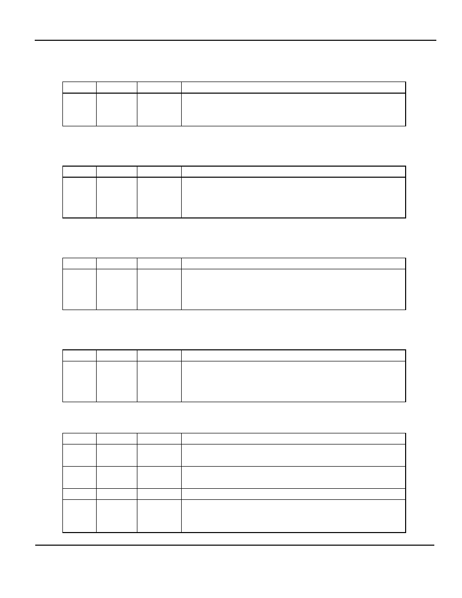
Wakeup Frame 3 Byte Mask 0 Register (Offset 0x0254): WF3BM0
This register contains the first 16 bytes mask values of the Wake up frame 3 pattern. Setting bit 0 selects the first byte
of the Wake up frame 3; setting bit 15 selects the 16th byte of the Wake up frame 3.
Bit
Default
R/W
Description
15 - 0
--
RW
WF3BM0
Wake up Frame 3 Byte Mask 0
The first 16bytes mask of a wake up frame 3 pattern.
Wakeup Frame 3 Byte Mask 1 Register (Offset 0x0256): WF3BM1
This register contains the next 16bytes mask values of the Wake up frame 3 pattern. Setting bit 0 selects the 17th byte
of the Wake up frame 3; setting bit 15 selects the 32nd byte of the Wake up frame 3.
Bit
Default
R/W
Description
15 - 0
--
RW
WF3BM1
Wake up Frame 3 Byte Mask 1
The next 16bytes mask covering bytes 17 to 32 of a wake up frame 3
pattern.
Wakeup Frame 3 Byte Mask 2 Register (Offset 0x0258): WF3BM2
This register contains the next 16bytes mask values of the Wake up frame 3 pattern. Setting bit 0 selects the 33rd byte
of the Wake up frame 3; setting bit 15 selects the 48th byte of the Wake up frame 3.
Bit
Default
R/W
Description
15 - 0
--
RW
WF3BM2
Wake up Frame 3 Byte Mask 2
The next 16bytes mask covering bytes 33 to 48 of a wake up frame 3
pattern.
Wakeup Frame 3 Byte Mask 3 Register (Offset 0x025A): WF3BM3
This register contains the last 16bytes mask values of the Wake up frame 3 pattern. Setting bit 0 selects the 49th byte
of the Wake up frame 3; setting bit 15 selects the 64th byte of the Wake up frame 3.
Bit
Default
R/W
Description
15 - 0
--
RW
WF3BM2
Wake up Frame 3 Byte Mask 3
The last 16 bytes mask covering bytes 49 to 64 of a wake up frame 3
pattern.
Chip ID and Enable Register (Offset 0x0400): CIDER
This register contains the chip ID, and the chip enables control.
Bit
Default
R/W
Description
15-8
0x88
RO
Family ID
Chip family ID
7-4
0x05
RO
Chip ID
0x05 is assigned to KSZ8841-PMQL
3-1
000
RO
Revision ID
0
-
RW
Start Controller
1 = Start the chip operation
0 = Stop the chip operation
发布紧急采购,3分钟左右您将得到回复。
相关PDF资料
PIC18LF24K22-I/SS
IC PIC MCU 16KB FLASH 28SSOP
PIC24F08KL402-I/ML
IC MCU 16BIT 8KB FLASH 28-QFN
PIC24F08KL302-I/SP
IC MCU 16BIT 8KB FLASH 28-SPDIP
PIC16LF1938-I/ML
IC MCU 8BIT FLASH 28QFN
PIC24F08KL402-I/MQ
IC MCU 16BIT 8KB FLASH 28-QFN
PIC16LF1938-I/MV
IC MCU 8BIT 28KB FLASH 28UQFN
PIC18F24K22-I/SS
IC PIC MCU 16KB FLASH 28SSOP
PIC16F1938-I/ML
IC MCU 8BIT FLASH 28QFN
相关代理商/技术参数
PIC16F639-I/P
功能描述:8位微控制器 -MCU 4kb 128 RAM 12 I/O RoHS:否 制造商:Silicon Labs 核心:8051 处理器系列:C8051F39x 数据总线宽度:8 bit 最大时钟频率:50 MHz 程序存储器大小:16 KB 数据 RAM 大小:1 KB 片上 ADC:Yes 工作电源电压:1.8 V to 3.6 V 工作温度范围:- 40 C to + 105 C 封装 / 箱体:QFN-20 安装风格:SMD/SMT
PIC16F639-I/SO
功能描述:8位微控制器 -MCU 4kb 128 RAM 12 I/O RoHS:否 制造商:Silicon Labs 核心:8051 处理器系列:C8051F39x 数据总线宽度:8 bit 最大时钟频率:50 MHz 程序存储器大小:16 KB 数据 RAM 大小:1 KB 片上 ADC:Yes 工作电源电压:1.8 V to 3.6 V 工作温度范围:- 40 C to + 105 C 封装 / 箱体:QFN-20 安装风格:SMD/SMT
PIC16F639-I/SS
功能描述:8位微控制器 -MCU 4kb 128 RAM 12 I/O RoHS:否 制造商:Silicon Labs 核心:8051 处理器系列:C8051F39x 数据总线宽度:8 bit 最大时钟频率:50 MHz 程序存储器大小:16 KB 数据 RAM 大小:1 KB 片上 ADC:Yes 工作电源电压:1.8 V to 3.6 V 工作温度范围:- 40 C to + 105 C 封装 / 箱体:QFN-20 安装风格:SMD/SMT
PIC16F639-I/SS
制造商:Microchip Technology Inc 功能描述:8-Bit Microcontroller IC
PIC16F639T-I/SO
功能描述:8位微控制器 -MCU 4kb 128 RAM 12 I/O RoHS:否 制造商:Silicon Labs 核心:8051 处理器系列:C8051F39x 数据总线宽度:8 bit 最大时钟频率:50 MHz 程序存储器大小:16 KB 数据 RAM 大小:1 KB 片上 ADC:Yes 工作电源电压:1.8 V to 3.6 V 工作温度范围:- 40 C to + 105 C 封装 / 箱体:QFN-20 安装风格:SMD/SMT
PIC16F639T-I/SS
功能描述:8位微控制器 -MCU 4kb 128 RAM 12 I/O RoHS:否 制造商:Silicon Labs 核心:8051 处理器系列:C8051F39x 数据总线宽度:8 bit 最大时钟频率:50 MHz 程序存储器大小:16 KB 数据 RAM 大小:1 KB 片上 ADC:Yes 工作电源电压:1.8 V to 3.6 V 工作温度范围:- 40 C to + 105 C 封装 / 箱体:QFN-20 安装风格:SMD/SMT
PIC16F648A-E/ML
功能描述:8位微控制器 -MCU 7KB 256 RAM 16 I/O RoHS:否 制造商:Silicon Labs 核心:8051 处理器系列:C8051F39x 数据总线宽度:8 bit 最大时钟频率:50 MHz 程序存储器大小:16 KB 数据 RAM 大小:1 KB 片上 ADC:Yes 工作电源电压:1.8 V to 3.6 V 工作温度范围:- 40 C to + 105 C 封装 / 箱体:QFN-20 安装风格:SMD/SMT
PIC16F648A-E/P
功能描述:8位微控制器 -MCU 7KB 256 RAM 16 I/O RoHS:否 制造商:Silicon Labs 核心:8051 处理器系列:C8051F39x 数据总线宽度:8 bit 最大时钟频率:50 MHz 程序存储器大小:16 KB 数据 RAM 大小:1 KB 片上 ADC:Yes 工作电源电压:1.8 V to 3.6 V 工作温度范围:- 40 C to + 105 C 封装 / 箱体:QFN-20 安装风格:SMD/SMT